Every year, thousands of students complete VLSI courses…
But only a few become industry-ready.
#Why?
Because most training stops at theory.
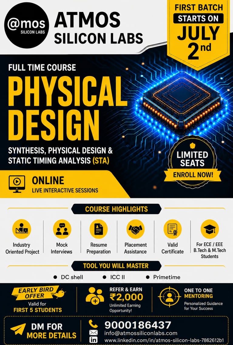
At Atmos Institute, we are starting a batch focused on what actually matters in the semiconductor industry:
🔥 Practical Tool Explosure
🔥 Continuous LMS support
🔥 Industry-oriented teaching
🔥 Interview-focused preparation
🔥 Placement Assistance
This is not just another course.
This is a serious step toward becoming a #PhysicalDesignEngineer.
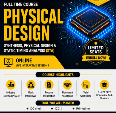
If you want to learn how chips are really built --> from Floorplanning to STA --> this batch is for you.
📅 Batch Starts: July 2nd, 2026
Limited seats for better interaction & mentoring
📩 Registrations are now open: https://lnkd.in/g3devv5C The semiconductor industry is expanding fast.
The right time to prepare is NOW.